Simple Class E Transmitter
Class E amplifiers are
very efficient amps and are generally built with
MOSFET transistors. The principle is to drive the
MOSFET's gate input with square waves to quickly put
the device into it's low ohmic region and to do this
when the voltage across the drain of the MOSFET is at
or near zero volts. This greatly reduces the heat
dissipated by the MOSFET and increases efficiency. A
choke value for the drain is chosen so that it
resonates at the operating frequency, in combination
with the parasitic capacitance of the drain and the
output filter. The "fly wheel" effect of
the resonant tank causes the drain voltage to drop to
zero before the MOSFET is switched back on.
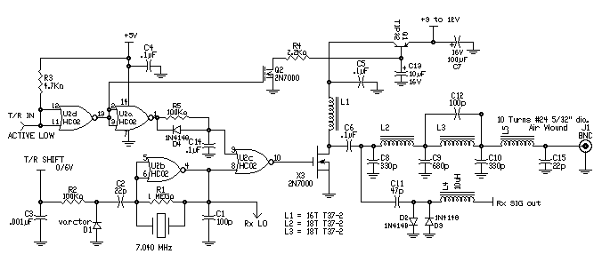
Efficiencies of 70% or more can be achieved this way. The circuit show below
is a simple Class E transmitter and is shown built
for 40 meters. It uses a 74HC02 NOR gate as a crystal
oscillator. The other three gates in the package are
used to gate the clock signal to the output MOSFET.
The crystal oscillator can also be used with a direct
conversion receiver. An Rx offset curcuit is shown to
shift the oscillator frequency when receiving.
A 2N7000 is used for
the final power amp. Although only one is shown,
three '7000's are used in parallel to reduce the
"on" resistance, which inproves efficiency.
70-75% efficiency can be achived. The amplifier
delivers about 2 watts output with a 9 volt supply
and about 4 watts with a 12 volt supply. The plastic
TO-92 2N7000's bearly get warm to the touch.
For best results the
spacing on the output filter inductors with need to
be "tweaked". Monitor the drain current and
output power and calculate efficiency. Adjust the
spacing of the windings on the output filter
inductors until you get the best efficiency. L2 will
have the greatist effect. L5 and C15 are used to
suppress VHF spurs, which aren't effectively
attenuated by the HF low pass filter.
If the square wave
drive to the fet is simply gated on and off, the
keying waveform is very steep and causes key clicks.
Therefore, the supply voltage to the PA needs to be
ramped up and down in order to provide for a least
some wave shaping. Q1 is a PNP power transistor which
is turned on and off by Q2. C19 slows the turn on and
turn off time down and causes the voltage on the
collector to rise and fall with about a 5 ms time
constant. R5 and C14 form a delay to keep the drive
active to the PA while the supply is ramping down.


No comments:
Post a Comment