Sunday 13 February 2011

Portable HF linear amplifier

 
Having got back on the air and started lots of portable operation with my FT-817, I have realised that quite often a little bit more power would not go amiss. I have started on a series of projects to get this power through the use of some simple, portable linear amplifiers. I was encouraged along this route by the publication of Eamon Skelton's "Homebrew" column in the July and August 2008 RSGB RadCom, which suggested an HF linear could be built using cheap MOSFET transistors - for me cheap is good.
Output transformer
The linear is a class AB push-pull design and needs a suitable broad band output transformer, which can easily be made using a couple of large ferrite chokes. The primary winding is a single turn, which is made as a tube using the braid from coax cable and copper clad board end pieces. Here are the bits:
transformer bits
It is easiest to assemble this by leaving the coax core in place whilst the braid is soldered to the end pieces; here the braid is pushed through ready for soldering:
transformer assembly
In this next stage, one half of the transformer is complete and the other side is ready for soldering. I forgot I had a 25W soldering iron stashed away which would have made this much easier than with my 15W Antex!
transformer assembly
Here is the transformer assesmbled, with the secondary winding threaded through the primary.
transformer assembled
Heat sink
Even a relatively low power linear needs a heatsink; efficiency is not going to be much better than 50% and it may well get run at higher powers than originally anticipated for portable use when it gets used car or caravan portable! I had a number of old heatsinks in the junk boxes, but wanted to be able to get the transistors inside the case; this needed a conductor and I decided copper bar would be best. Blake's metal centre got hold of come lovely stuff for me; I now have enough to see me out.
heat sink bits
I needed to tap a couple of holes to take screws to hold down the transistors. Having no handy taps available (must get one before I next need to do this) I made a couple from some steel screws by filing flats near the end. This works absolutely fine since copper is so soft, providing you use plenty oil for lubrication.
heat sink taps
Here you can see how the copper bar is brought through a slot in the box, with the heatsink mounted on the outside. The screw standoffs are to mount copper clad board to take the components. The bar also has a shallow hole to take a thermistor for a bit of thermal feedback on the bias.
heat sink in place
Testing the basic design
For the initial design I intended to use IRF740 MOSFETs since these seemed to have suitably huge power characteristics. Before putting in the transistors though, I assesmbled the output and input broadband transformers onto the copper clad boards. No PCBs for this project - the basic circuit is very simple and can mostly be put together with point to point wiring. The initial PA circuit was basically that given by Eamon Skelton in the Homebrew column in RadCom, July 2008, which used IRFP260 FETs.
boards in box
The MOSFETs need DC bias, and this is set up on a subsidiary stripboard using a 5V regulator and trimpot. The stripboard also carries a relay to turn the bias on when PTT is active on the transceiver; this saves power during receive. Here is one transistor in place. However, extensive testing ended up with me being unable to cure instability with the IRF740; even with just one transistor in place, the thing generated RF at several unwanted MHz! Its characteristic is very steep, so this is not too surprising; rather than spending more time on it I decided to try some IRF510 MOSFETs instead, since these have been used successfully in a number of small linears like this.
first transistor in
The IRF510s were nice and stable, but it proved hard to get a lot of power out of them with the original design. Eventually I swiped some ideas from a circuit by Mike Cossor WA2EBY (QST March 1999) - also the Packer amplifier described by Virgil Stamps K5OOR (2007) which is essentially the same circuit. These are (a) a better input transformer arrangement, and (b) a better HF choke arrangement to feed the MOSFETs. The photo below shows the amp at this stage, ready for a rebuild. 
revised assembly
The redesign looked pretty good, and put out over 60W RF into the dummy load at 3.5MHz using two 12V SLABs to give a 24V supply and using 2.3W input, though some of that power is in the harmonics. I will probably not drive it quite so hard for portable use.
Rebuild
Here's the rebuild underway; the original input transformer has been removed but the bias circuitry is in place. The output transformer has been moved closer to the FETs.
partly rebuilt
Once the rebuild was done apart from the low pass filters (I had just ordered the toroids from Heros Technology - excellent service!) I wanted to try it out since we were off for the weekend. I thought I might get by with an 80m LPF made using ferrite toroids I happened to have instead, but unfortunately a sniff of full power RF from the amp fried the first toroid. Reassuring in some ways in that it proves there's a fair amount of power there!
The photo below shows everything in the box - at least, except for the topband and 10m bandpass filters. The filter board is in the top right, switched manually centre right, and the input and output relays are now in place. The new input transformer is much neater and the HF choke for the FETs is counter wound as in the Packer Amp. The TX control lead from the FT-817 is also made up and plugged in on the left just above the input BNC socket. The treacle tin dummy load is now filled with out of date veggie oil which should stop the resistors frying. The iron dust toroids don't even get warm under full power, thank goodness! Signals all look pretty clean on the scope with the linear driven using an FM carrier, and look fine with SSB as well, though I must build a two tone test oscillator. It appears to be able to produce 35W out for 2.5W in easily enough over the lower bands - can't go much higher than that for portable as I have to carry the batteries.
fully rebuilt
Here's the finished product (almost) - it still needs some rubber feet in case it spends time on the XYL's best table at the caravan, and the innards still need the LPFs for 160m and 12m/10m. On this end are the BNC connection to the transceiver, the mini DIN connector to the PTT signal on the data in/out on the transceiver, an LED to indicate transmit (i.e. FET bias voltage on and relays switched), and the 4mm power connectors. 
fully rebuilt
At the other end we see the band switch, and the BNC connector for the antenna. The copper bar connecting the FETs to the heatsink (thermally) can also be seen down the tunnel in the heatsink. I have another of these - they were bought as a pair for a Hi-Fi amp that never got completed - we bought one instead! The other one will probably be used for the 6m linear once I get that started.
fully rebuilt
As of March 15 2009 it has been on the air - I did a SOTA activation on Cairnpapple Hill with great success using an inverted 'V' with the apex at 6m (fishing pole) and the ends about 1m off the ground - I use garden canes to support the strings at the ends. Made about 25 HF contacts (the bulk of these after being "spotted" on the SOTA website) but included the De Havilland Museum special event station in Hertfordshire and my first European mainland HF contact in Belgium. The weekend after I operated at the caravan in south west Scotland on 40m with a quarter wave vertical (on the Spiderbeam 12m pole) - it was the Russian DX contest weekend and so I picked up several eastern European contacts. The following morning I set up near the shore operating on 80m with a full size inverted V on the Spiderbeam pole. It has received quite a few favourable reports as to signal quality so I'm very pleased with it and will play a lot more with it in the future - I can have some fun experimenting with HF aerials.
Circuits
This is the main part of the rig - basically the Packer amp circuit referred to above, which is online in the HF Projects website construction manual.
PA circuit
The input to the PA has an attenuator to match the FT-817's output.
PA circuit
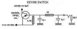
Here's the relay TX switching and bias circuit which is driven off a 5V regulator and has some thermal compensation. Not likely to be much of a problem where I normally operate - in the cold wind on the top of a Scottish hill! I needed to add the 0.22µF capacitor on the TX input switch as the relays started chattering when in use on 20m - clearly detecting and being overpowered by RF.
PA circuit
The power input allows for a range of supply voltages, since there's a 12V regulator for the relays. It still works fine with 12V input, though the output power is then somewhat limited.
PA circuit

QRP antenna tuner circuit


Low power ( 3 to 30 MHz) transmitters constructed by hams are generally called QRP’s. For such transmitters a well tuned antenna is a must.If the impedance is not properly matched there will be a little or no output.But if properly matched there will be great results.A circuit for matching the antenna properly with the transmitter id given below.
The output of the transmitter is given to the input of the tuner( connector BNC1). The output of the tuner(connector BNC2) must be connected to antenna.Then adjust the L1 and C1 to obtain the maximum transmission power.The transmission power can be checked using a SWR meter.

15 METER VXO-TUNEDCW TRANSMITTER

An easy-to-build and affordable CW rig that puts out about 500 milliwatts on15 meters, this simple modification of W7ZOI's classic two-stage "Universal QRP Transmitter" (also known as the "Little Joe" ) features a VXO circuit that "warps" each crystal frequency by as much as 10kHz or more for increased flexibility. This transmitter's oscillator runs throughout the transmit period; voltage is keyed to the amplifier section while the oscillator is on. After construction,tuneup is a snap: connect a 12-15 VDC power source and 50-ohm dummyl oad or RF wattmeter and tune a monitoring receiver to the anticipated transmit frequency. Flip on the oscillator switch and adjust C3 until a tone is heard on the receiver. Play with C1and notice the shifting of frequency (the crystal frequency DECREASES asC1's capacitance INCREASES). Depress the key and adjust C3 for maximum output. Tuneup adjustment is now complete. Hook up an appropriate antenna (a 40-meter dipoleworks great on 15 meters without use of a transmatch or antenna tuner)and there you go - bring on the sunspots!

Unless otherwise noted, decimal capacitance values are in microfarads(uF);

whole-number values are in picofarads (pF or uuF).

s.m.=silver mica.

* = see below.

C1 - 50pF air-variable capacitor mounted on front panel.
C2 - 10pF trimmer capacitor. OK to use 2pF-8pF fixed capacitor instead. Limits the VXO range and prevents the crystal from "running onits own."
C3 - 60pF mica trimmer capacitor.
L1 - 17 turns #24 enamelled wire on Amidon T50-6 core.
L2 - 3 turns #24 enamelled wire wound over L1 in same direction.
L3 - 9 turns #22 enamelled wire on Amidon T50-6 core.
Q2 - NTE311, 2N3866, 2N3553, RCA4013, or similar NPN RF power transistor. Use heat sink.
Y1, Y2, Y3.... - Fundamental-mode crystals for desired frequencies.
15uH choke - I used a miniature RF choke, but W7ZOI recommends30 turns #28 enamelled wire wound on an Amidon FT37-63 core.
Misc. - Chassis box, rotary switch for the crystals OR a crystal socket for manual crystal switching, SPST switch for the oscillator, knobs(vernier dial for C1 recommended), hookup wire, RG174 miniature coax, solder,mounting hardware, etc.

Construction: I used my usual experimenter's circuit board available from many sources including Radio Shack. Keep all leads short as possible and use RG174 miniature coax for runs that carry RF. Mount the circuit board with the oscillator section & crystals close to C1. Use as manycrystals as you wish to spend the money for - I use three: 21135, 21150,and 21165 kHz which with the VXO covers the middle of the 15-meter Novice subband.

If your station setup doesn't have a filtered keyed-out +V capability from a station controller or other device, the transmitter will also needthe simple KEYING SWITCH depicted below.

To include the keying switch, connect the keying switch's +12-15 VDC tothe "+12-15 VDC" terminal of the transmitter's oscillator switch and thekeying switch's KEYED +V OUT to the transmitter's "KEYED-IN +12-15 VDC."A plug from the key is then connected to a jack mounted on the front panel.

20M 4W QRP Transmitter


2.5 W FM Power Amplifier


This rf power amplifier design for a 2.5 Watt power amplifier for the FM band. An input of 50 mW gives a final output power of 2.5 Watts with a 13 Volt supply. The best bit is that the amplifier requires no tuning once it's built - it gives roughly the same gain and output power right across the FM band from 88 to 108 MHz.


There's even some hefty output low pass filtering to make sure that harmonic output is small and no interference is caused to users (mostly military!) on multiples of the FM frequency being amplified. A nice design based on, believe it or not, a military one...!
Source
: ZFM

1W AM Transmitter


This AM transmitter circuit provides a nice, clean output of about 1 Watt (carrier power). Though designed for the medium wave band (circa 1.5 MHz) it would work equally well on higher frequencies (6.2 MHz for example) with a few tweaks in component values (see table on left - C15 should be adjusted for maximum output).


The carrier (produced by the 4049) is modulated at low-level by the MC1496 balanced modulator. There are then a couple of stages of linear amplification to reach the final output power so no modulation transformer is required. TR2, TR5 and TR6 are BC108 or similar; TR3 is a 2N3053 or 2N4427 or 2N3866 or any low/medium power NPN transistor. The main output transistors, TR4 and TR5 were originally 2SC1162 but BD135 or BD139 or other medium power RF transistors will do equally well. T1 uses a pre-tuned TOKO KANK3334 coil, the other transformers are wound on the red T50-2 toroids (the number of turns shown is the ratio, use about 4 to 5 times that number in reality - less at higher frequencies). The LED lights up if current in the output amplifier goes too high, so it's a kind of 'high SWR' warning.


Source: ZFM

250mW FM Power Amplifier

 
This project is a simple 2-transistor VHF power amplifier, with about 16dB gain, and requires no tuning or alignment procedures. Wideband techniques have been used in the design and the circuit is equipped with a "lowpass" filter to ensure good output spectral purity. The project has been designed for assembly on a single-sided printed circuit board. The circuit is specifically designed to amplify the output of 7mW to 10mW WBFM transmitters (wide band) to a final level of 250mW to 300mW, after the filter.


The first stage (Q1) operates in Class-A. Although Class-A is the least efficient mode, it does offer more RF gain than other clases of bias, and Q1 is a low-level stage, when compared to the higher power Q2 stage. The output of this stage is around 70mW of RF power. The stage is untuned so that it gives a very broadband characteristic. The transistor is biased by means of R5, R6 and L6, and the residual (standing) DC current is set by R4. The input signal is coupled by C9 to the Base of the transistor. Q2 is operated in Class-AB which leads to greater efficiency, but the RF gain is only about 8dB, but it amplifies the output of Q1 to typically 250mW. Q2 is biased by means of R3, R2 and L4. The input signal from Q1 is coupled to the Base of Q2 via C7.
The voltage regulator Q3 (78L08) is used to regulate the supply voltage to Q1 and the bias votages to both Q1 and Q2 so that the output RF power is relatively constant, even with large variations of supply voltage. Q3 also removes supply ripple as well as providing power for an FM transmitter like Kit 3018 wireless microphone ith the required DC 8v power.The output of the amplifier is filtered with a low-pass filter to reduce the output spurious and harmonic content. The output filter consists of C3, C4, L1 and L2.
COMPONENTS
Resistors 5%, 1/4W, carbon:
10R R1 brown black black
22R R7 red red black
47R R3 yellow orange black
120R R4 brown red brown
470R R2 yellow violet brown
2K2 R5 red red red
4K7 R6 yellow violet red
2N2369 Q1
2N4427 Q2 1
Ceramic caps
33p C3
47p C4
1n C5 C6 C7 C8 C9
10n C1 C11
Ecaps:
220u/16V C2
10u/25V C10
78L08 Q3
RFC L4 L5 L6
Ferrite L3
3 turn coil L2
5 turn coil L1
2 pole terminal block
HS106 heatsink (download documentation)

Wireless Microphone


clip_image002

Probably the most basic transmitter is a simple wireless microphone. This device may be used to connect a microphone to an audio or PA system without the interven-ing cable, which is a hazard in many situations. The wireless mike is a simple transmitter that acts as a one-way radio link to a nearby FM receiver. The output of the FM receiver then feeds the audio or PA system, replacing the wired microphone. Professional-grade mikes of this sort use a crystal-controlled receiver and transmitter operating outside the FM broadcast band at frequencies specifically intended for this

service. (Frequencies around 170 MHz are commonly used for this purpose.)A typical circuit of a wireless microphone is shown in Figure 3-1. It consists of an audio amplifier that feeds audio into the bias network of a free-running oscillator cir-cuit operating in the FM broadcast band. An electret microphone feeds audio into audio amplifier stage Q1. R1 biases the mike and may be varied to suit the mike used. This value is normally specified in the manufacturer’s data sheet, but 4.7 K is a good “generic” value if no data are available for the microphone. Audio is coupled via C2 to the base of Q1, which is biased by R2, R3, and R4 to about 4 volts and 0.5 milliamps. A low-noise, high-gain audio transistor, such as the 2N3565, should be used, but most high-gain, low-current transistors of this nature should work fine. Amplified audio at the collector is coupled through the RC network C3 and R5 to the base of oscillator Q2. Q2 acts as a grounded base oscillator, with feedback provided by C8. R5 and R6 provide starting bias for the oscillator transistor, and R7 provides emitter bias.

A VHF transistor, such as a 2N3563, 2N5179, or MPSH10, can be used for the oscillator, and any good 500-MHz or better NPN transistor should work, although the modulation characteristics may vary somewhat. Transistors with larger geometries or lower frequency ratings tend to have larger capacitances, with possibly somewhat better modulation capabilities, so do not think that a higher-frequency transistor than you really need will perform better. Tank circuit L1 C6, along with stray circuit and transistor collector-to-base capacitance, determines the frequency of oscillation. The collector-to-base capacitance is a function of collector-base voltage, and this voltage is modulated by the applied audio from R5, causing directfrequency modulation of the oscillator frequency. Because the oscillator power out-put also varies with collector voltage, some AM component will also be present, but this creates little harm in this application and is the price paid for simplicity. L1 is

typically tapped at 10–30 percent total turns from the RF ground end (Vcc rail or C9 in this case). The tap should be as close to ground as possible consistent with good signal output because the closer the tap is to the collector, the more effect the antenna will have on pulling the transmitter frequency. This effect is undesirable and can make the transmitter difficult to set on frequency. C6 is typically a 5- or 7.5-mm polyethylene or Teflon trimmer and is used to set the oscillator frequency. Its value is typically 3–5 pf per meter of operating wavelength.Because the FM broadcast band is approximately a 3-meter wavelength (100 MHz), C6 would be approximatley 9–15 pf. A 10 pf capacitance would be about right because the transistor and stray capacitances will be approximately 2–5 pf. Alternately, C6 can be made fixed and L1 varied via a slug or by stretching and squeezing turns, but this technique might be awkward for some applications, so the variable capacitor may prove to be a more practical method of frequency setting. The antenna is usually made about one-tenth of a wavelength at the operating frequency,

and at 100 MHz, is about 30 cm (approximatley 1 foot) long, but length also depends on application, mechanical constraints, allowable signal strength for meeting legal or FCC regulations where applicable, and the transmitting range desired. C7 is used as a DC-blocking capacitor and is generally around the same value as the tank-tuning capacitor. These values are only rules of thumb and provide working values for components, but final values should be calculated for optimum performance or determined empirically on working models.

Telephone “bug” Transmitter


clip_image002

A circuit for a telephone “bug” is shown in Figure . Again, the RF portion is identical, but the method of powering the circuit and the audio input circuitry is different. This unit is designed to be directly powered by the voltage available from the telephone line, with audio being fed to the circuit directly from the telephone line. How this is achieved can be seen in Figure 3-3. The circuit consists of a basic VHF oscillator tuned to a frequency in the FM broadcast band. In most telephone systems, a two-wire loop that connects the subscriber to the central office is used, with the loop current around 20 mA and the loop voltage usually 48 volts DC. When the phone is on the hook, it appears as an open circuit, and the full 48 volts is present on the line. (The actual voltage may vary somewhat.)When the telephone is taken off the hook, the voltage across the phone drops to a much lower value, around 5–10 volts, and a current of nominally 20 mA will flow. Superimposed on this line are audio and tone signals. In addition, an AC ringing voltage of around 100–120 volts at a frequency of 20 Hz may be supplied by the central office to actuate the ringer in the phone when a call is received. This “bug” can be placed in series with the hot leg of the telephone line. The DC line current may be used to derive a voltage for powering a small circuit such as the transmitter shown.R1 and a diode bridge D2 to D5 are inserted in series with the line, ensuring correct DC polarity. R1 shunts excess current around the circuit and passes 8–9 mA, about half the normal off-hook line current. C1 is an RF bypass that prevents strong RF signals accidentally picked up by the phone line from being detected in bridge D2 to D5, and thus appearing as audio on the phone line.

The voltage drop is regulated by zener diode D1 to 9.1 volts and filtered by C2. R5 is placed in series with the DC supply to sample the audio signal on the line and should be as low in value as possible. Line audio voltage drop across R5 is fed via C2 to the oscillator circuit, which is similar to that used for the wireless mike and is also tuned identically. This voltage causes frequency modulation of the oscillator operating in the 88- to 108-MHz FM broadcast band. Bridge rectifier D2 to D5 causes about a 1.3-volt drop. The total voltage drop from this circuit is 11–12 volts. This is about one-quarter of the available open circuit voltage and should not cause any problems in most instances. This “bug” can be easily detected by a knowledgeable technician because of the high off-hook circuit voltage present on the phone line. This voltage is approximately 16–22 volts, which is 11–12 volts higher than that normally encountered (5–10 volts); however, this circuit has the advantage of not having a battery that must be replaced periodically. The antenna can be a short (6-inch) wire, or the telephone line itself can be used as an antenna.

Broadband RF Power Amplifier 1.8-30 MHz


Here's RF Power Amplifier for QRP with low cost. This circuit is a broadband one from 1.8 to 30 MHz, so it is "no-tune" and you need only to regulate the quiescent current bias multiturn trimmer of each Mosfets couple. This means also low efficiency (for a lower IMD it is even low as around 20-30%) together with good heat sink + blower system.

HF QRP Linear Amplifier with 2x 2SC2166 + 2x 2SC1969  Push Pull Transistors (13.8V)

The push-pull configuration permits to get a better attenuation of even harmonic frequencies (a good benefit since the second is the closer 2x fundamental freq.). The output stages have 2 separate transformers in each couples so the power supply current does not flow in to the output transformer to avoid saturation and the floating winding helps for balance for harmonic attenuation and stability.

HF QRP Linear Amplifier with 2x IRF510 + 2x IRF510 Push Pull Low Cost Mosfets (28V)

We have emploied also in this low power unit the circuit found in higher power units to stabilise thermically and regulate the bias current around a trusted LM723 IC, the transistors are used only for PTT control. In the first stage Mosfet couple we have used a feedback circuit to optimize gain-frequency response. Without it the low frequency gain is very high, too high: at 3 MHz 50 dB ! and a lower 30 dB at 30 MHz, but with this feedback circuit the overall gain variation is close to a +/-3 dB, a good result.

We tried a similar feedback in the output couple but results where a poorer IMD performance so it has been omitted. We selected Mosfets couples in a simplified way (while not so precise RF matching practice) measuring drain-source resistence: a better way could be to measure in a simple test circuit current drain at a given gate voltage applied for all devices and choose the ones that showed closer current values.

Simple AM transmitter


clip_image002

A simple AM transmitter of this type is illustrated in Figure 3-5. The transmitter consists of oscillator stage Q1 and modulator/buffer stage Q2. Q1 is biased via R1, R2, and R3. L1, C3, and C4 form the tank circuit with feedback network C3-C4 providing feedback to the emitter of Q1. RF voltage at the junction of C3 and L1 drives buffer/modulator stage Q2. Q2 is biased by base current produced by RF rectification in the base emitter junction of Q2. C6 is an RF and AF bypass capacitor. C9, C10, and L2 form the tank circuit for the collector of Q2. RF is taken from the junction of C9 and C10 and fed to a shortwire antenna. Audio is fed to modulator Q2 via C8 and isolation resistor R5 and mixes with the RF signal in the collector circuit of Q2, producing a signal that has sum and difference frequencies if the RF carrier and AF input (upper and lower sidebands) along with the carrier signal. An AM signal appears at the collector of Q2. Audio with an RMS voltage equal to about 0.7 times the collector voltage of Q2 is needed for full modulation of the output.Because of the high level of audio needed, the modulation obtained from this circuit is somewhat limited with conventional audio sources because several volts of audio into a few hundred ohms is needed. The circuit demonstrates the principle of an AM transmitter, however, and with a suitable audio drive level, produces a wellmodulated AM signal.

L1 and L2 are chosen to resonate with the circuit capacitances of about 150 and 165 pf, respectively, and in the test circuit, inductances of 400–500 microhenries were used to obtain the desired 600-kHz output frequency, but this circuit can be operated anywhere in the AM band with suitable inductors. For operation at 1500–1700 kHz, for example, adjustable inductors having a range of 50–100 microhenries would be suitable.

VFO Controlled FM Transmitter


clip_image002

Examining the schematic diagram shown in Figure 6-1 shows that the transmitter consists of three stages: an audio amplifier, a voltage-controlled oscillator (VCO), and a buffer amplifier. The audio stage takes the audio input in the 20–15000 Hz range and amplifies it by a factor of about five times, and increases in gain at 6 dB/octave above 2.1 kHz to add the needed preemphasis to the audio. This audio is fed to a VCO consisting of a Colpitts oscillator with a varactor diode acting as an FM modulator, and the VCO feeds a buffer stage to bring the output up to about 0.5 mW, which will produce a usable signal up to about 200 feet with a short (6-inch) whip antenna. A zener diode provides a fixed 6 volts to the VCO for improved stability with declining battery voltage. Nine to twelve volts is recommended, although the transmitter will operate down to six volts, but the zener regulator will not function properly at this voltage, and more drift may be expected.

Referring to the circuit diagram, audio input is applied at coupling capacitor C1 and ground. Audio is fed through R1 to audio stage Q1, whose gain is determined by the ratio of R4 and R2 to R1. C2 provides bypassing above 2 kHz, reducing the feed-back and increasing the gain as frequency increases; this provides preemphasis. R5 and R3 are bias resistors. Audio appears at the collector of Q1, amplified about five times. This audio is fed to gain control R6 through C3, and potentiometer R6 sets the deviation or modulation level. Audio from the wiper of R6 is fed through C4 and isolation resistor R7 to the varactor-modulator diode D2. D2 is reverse-biased through R8 with about 6.8 volts reverse bias. This sets the capacitance of D1 to about 15 pf.

D1 is a 6.8-volt zener diode, with C6 and C7 acting as bypass capacitors to reduce noise and provide an RF ground. The VCO consists of Q2 with associated bias resistors R10, R11, and R12. The VCO is a Colpitts oscillator configuration. This setup has the advantage of reducing the loading on the oscillator frequency-determining circuit by the indefinite and variable transistor parameters, reducing drift caused by the transistor. It is an excellent oscillator when low drift is desired because the transistor input impedance is swamped out by relatively large capacitors C10 and C11.

The series combination of C11, C12, L1, and trimmer C9 in parallel with C8 form the main oscillator “tank” circuit. L1 is adjustable with a slug to set the coarse frequency, and C9 is used for fine adjustment.The varactor diode appears in series with C5, and the total capacitance of about 3.5 pf appears in parallel with C8. Adding this 3.5 pf to the 22 pf of C8 and thenominal 6 pf capacitance of C9 (variable from 2–10 pf ) totals about 31.5 pf, which appears in series with the series combination of C10 and C11 (41 pf ). This provides a total effective capacitance of about 18 pf, and L1 tunes with this capacitance. It can be shown that the variation of C10 and C11 caused by the transistor capacitances has only a small effect on the tuned frequency. This contributes to frequency stability.

Audio on D2 varies its capacitance, which varies the capacitance of the tuned circuit, causing frequency modulation of the oscillator, with very little AM component. This will be much smaller than that which would result from modulating the VCO transistor Q2 directly in order to vary its collector capacitance. Oscillator output from a low impedance point (across C11) is fed through C22 to buffer stage Q3. R13, R14, and R16 provide bias for Q3, while R15 suppresses possible UHF self-oscillation in Q3.

C13 is an RF bypass, and the output is filtered by tank circuit L2, C15, and C16. RF output is taken from the junction of C15 and C16 and is about 0.5 mW into 50 ohms.

Coil data is given in Figure for the construction of L1 and L2. They are not critical, and the coils may have to be adjusted later by adding or removing a turn to obtain operation on your chosen frequency. You can find suitable slugs in the IF and video coils used in older TV receivers and junked CB radios. Data shown is for the low end of the FM band (88–92 MHz), where there is apt to be less competition from higher-power commercial stations. Do not operate near and never, never above 108 MHz because you could cause interference with aeronautical navigation systems.

6W RF Power Amplifier with 2SC1971


This RF Power Amplifier taken from FRB Amplifier Kit. It uses 2SC1971 for FM broadband design from 88 to 108 MHz.

Power Amplifier Schematic Circuit

Power Amplifier Printed Circuit Board and Component Layout

Assemble Instructions
RF power amplifier assemble by soldering the components to the pads indicated. Keep coil, resistor, and capacitor leads as short as possible. The coils should be 3/16" to 1/4" above the board and separate turns by one wire diameter. Bend leads to form a little mounting foot for soldering to the circuit board.


Tuning and power output are affected by the distance between the coil turns, you can make fine adjustments by either spreading or compressing the coil slightly. The area surrounding the pads is ground. C2, C3, C4, C6, C7, C8, C9, C10, L2, and R1 are soldered at one end to ground as well as the shield braid on the coax cables. Bolt Q1 to a small heat sink or the chassis with heat sink thermal compound or gray thermal pad underneath the tab. With an input level of 200-500mw, you should see an output of 5-6 watts. Be sure to have a proper dummy load (50 ohms) or tuned antenna connected to the output, doing otherwise will likely destroy the transistor.

RF Amplifier Broadband 88-108 MHz 20W


This RF amplifier for FM 88-108 MHz with no tune (broadband) needed to cover all the FM Band. This RF Power amplifier is equiped with two Philips bipolar transistors : the BLV10 & BLW87.

All the impedance networks (Input-Output) of this RF amplifier have been determined by using the softwares: Mimp.EXE.

This RF Amplifier need a 9 elements low pass filter ensures that its harmonic frequency meet at least a 60 dB rejection from the carrier.(RF Simulation with RFSIM99)
This RF FM amplifier has a 21 dB gain with a 55 to 65% efficiency.
RF Power Amplifier PCB Layout

60W Linear Amplifier with IRF840

 
This is a RF Linear amplifier for QRO using power mosfet IRF840 with power out 60 Watts. It's simple all solid state circuit. The IRF series of power transistors are available in various voltage and power ratings. A single IRF840 can handle maximum power output of 125 watts. Since these transistors are used in inverters and smps they are easily available for around Rs: 20/-.
The IRF840 linear amplifier can be connected to the out put of popular VWN-QRP to get an output of 60 Watts. The circuit draws 700 ma at 60 Volt Vcc. Good heat sink is a must for the power transistor.
Alignment of the Linear Amplifier
Connect a dummy load to the out put of the circuit. You can use some small bulb like 24V 6 Watts as the dummy load. I have even used 230V 60 Watts bulb as dummy load with my IRF840 power amplifier working at 120Volts. Adjust the 10K preset to get around 100 ma Drain current. I used gate voltage of 0.8V with my linear amplifier. A heigh gate voltage can make the power transistor get destroyed by self oscillation. So gate voltage must be below 2V and fixing at 1V will be safe.Bifilar transformer T1 is wound with 8 turns 26SWG on 1.4 x 1 balun core. The coil on the drain of IRF is 3 turns 20 SWG wound on 4 number of T13.9 torroids (two torroids are stacked to form a balun core). The RFC at the Vcc line is 20 Turns 20 SWG wound on T20 torroid.

5 W transmitter power amplifier 88-108MHZ


The power amplifier can be reactive 1-2 W ,88-108MHZ power FM transmitter As for the expansion of 10-15 W, a single C Larger and multi-level low pass filter components, has a high conversion efficiency and strong Yi-wave suppression.

Circuit see attached map shows, using high-power launch of C1972, its parameters are as follows: 175 MHZ, 4A, 25W, power gain ≥ 8.5 db, as shown by parameters, circuit work center frequency of about 98 MHZ, the importation of about 2 W of RF power , The rated output up to 15 W.

To maintain 88 ~ 108 MHZ with any frequency output reached rating, according to the level before the center frequency of some components to make suitable adjustments. May, when necessary, to reduce low-ball-series, to increase power output. The expansion of the power signals from three low-pass filter Yi-filtered high element of the transmitting antenna feed.

Components choice: In addition to electrolytic capacitor, the other tiles with high-frequency capacitors, C11, C12, C14 use high-frequency characteristics of a good, stable performance of adjustable capacitors, inductors Choke RFC1, RFC2 finished with inductors, must pay attention to the current RFC2 Carrying capacity, should use the coarse diameter Cores with the inductors.
L1-L6 available ø0.8mm the high-intensity enameled wire system, a diameter of about 5 MM, a few laps in the plans to "T" for the units indicated. Q1 ordinary Q9 socket, and supporting the use of plugs. Q2 used for 50 Ω RF output connectors, and then of resistance is smaller, more conducive to impedance matching.Larger effective power more common for the launch of the C1972, of course, especially if you sufficient money to buy blocks C2538 contour of the gain, power will be even greater.

Debug circuit, be sure to pay attention, the power circuit, we must connect false load (I use 30 1 W, 1500 Ω high-precision metal film resistors made parallel), and there must be enough in the cooling devices, normal working hours Power Of not less than 2.5 A, the antenna impedance strictly equivalent to 50 Ω, can not be used Duanbang drawbars antenna, or a strong current of RF feedback circuit will create their own interference, most of RF energy to space and can not be convergence in the consumption of power, to overheating Damage must be launched for 50 Ω coax, tabled Reply to launch outdoor antenna.

Circuit the normal work of the key lies in whether the circuit debugging, the whole process had to very carefully.Debugging, enter only the smaller the incentive power supply voltage drop to 9 V, using high-frequency voltage (can not use ordinary multimeter) monitoring false load at both ends of high-frequency voltage value, regulating C12, C14, L3, L4, L5, L6 So that the voltage range of 15-20 V around, and then adjust C11, L1 voltage to the largest.

And then gradually raise the voltage, each raising a voltage repeatedly adjusted C12, C14 and C11, L1 so that the maximum output voltage, noted that the input voltage and RF power simultaneously increasing incentives to ensure the accuracy of the results of debugging. Reach rating, 13.8 V supply voltage of about 2 A current work around, 50 Ω-load resistance at both ends voltage ≥ 40 V, RF power output of 15 W.

With the RF power amplifier with 50 Ω-wide umbrella to the vertical launch antenna (gain of about 2 dB), to ordinary FM radio test fired from the coverage of not less than 15 KM

NOGAnaut 80M Transmitter


The crystal oscillator is the simplest form of transmitter. Normally, oscillators are used to drive buffer amplifiers and power amplifiers, which provide increased output, as well as prevent the output circuit from adversely loading the oscillator.

Most transistors exhibit a characteristic impedance different from the 50-ohm impedance of a well-tuned antenna system. An improper match between the impedance of the transistor and the load (e.g. antenna system) can cause severe power degradation, and worse, can seriously affect the signal, including shifting the oscillator frequency in unpredictable ways.

In the NOGAnaut transmitter, the 2N2222A transistor, which exhibits a characteristic impedance of approximately 200 ohms, is matched to a 50-ohm load via the pi-network filter composed of C1, C2 and L2. The values of these components were chosen to provide a close match between the 200-ohm transistor and a 50-ohm antenna (it is therefore critical that a good 50-ohm antenna system be used with this transmitter). It so happens that these values also form the familiar half-wave harmonic filter, thus satisfying FCC spurious emissions requirements.

clip_image001

Figure 1. NOGAnaut 80M Transmitter Schematic.

Capacitor C5 provides the necessary feedback to begin oscillation. You may find that you can operate your NOGAnaut without this capacitor--stray capacitance in the circuit provides a certain amout of feedback without C5. However, it was found during development of this circuit that the oscillator can have troubles starting at times, therefore it is recommended that you leave C5 in the circuit.

POWER METER


This Power meter is capable of dissipating up to 100 watts for a short period and 20 watts continuously. You will need 20 1K ohm resistors connected in parallel, the resistors should be 1 watt.

To set up calibration:

Adjust the 47k for the low power range against a calibrated power meter, then adjust the 470K for the high power range against a calibtated power meter, do not re-adjust the 47k on high power.

SHORTENED DIPOLE


To construct each side of the antenna proceed as follows. Cut a 10.25 metre length of 24/0.076 insulated wire, and a 160 mm length of 40 mm o.d plastic tubing ( white plumbers tubing). Measure a 2.75 portion of the wire and attach the wire to the plastic former. Wind 40 turns of the wire onto the plastic former, and firmly secure the end of the winding. Make the other half of the antenna in the same way. Attach the ends of the 2.57 metre sections to a suitable centre insulator, which should also mount the choke balun, connect the 50 ohm coax, then carefully waterproof the whole assemby.

The choke balun uses RG174AU coax and a 40mm Ferrite Toriod.

Once the antenna is errected adjust it to resonance on 7.030Mhz by folding back the ends, and adjust the length to provide minimum SWR.

Article from SPRAT Issue 74 Spring 1993