Tuesday 22 March 2011

NiMH Battery Charger


Here is a simple battery charger for the Nickel Metal Hydride battery that requires current regulated charging. The charger provides 140 mA current for quick charging of the battery.Power supply section consists of a 0-18 volt AC 1 Ampere step-down transformer, a full wave bridge rectifier comprising D1 through D4 and the smoothing capacitor C1. Current regulation is achieved by the action of R1,R2 and the Epitaxial Darlington PNP transistor TIP 127. Resistor R1 keeps the charging current to 140 milli amperes. LED and resistor R2 plays an important role to control the base current of T1 and thus its output.


Around 2.6 volts drop develops across the LED which appears at the base of T1. Emitter – base junction of T1 drops around 1.2 volts. So 2.6 – 1.2 volts gives 1.40 volts. So the current passing through R1 will be 1.40 V / 10 = 0.14 Amps or 140 Milli Amps. The LED act as the charging status indicator. LED lights only if the battery is connected to the output of circuit and the input voltage is normal.

Read more: http://electroschematics.com/6073/nimh-battery-charger/#ixzz1HL7dzmz5

10-M DSB QRP TRANSMITTER WITH VFO


NE602 circuit : 10-M DSB QRP TRANSMITTER WITH VFO
NE602
NE602 circuit : 10-M DSB QRP TRANSMITTER WITH VFO
NE602
The three schematics represent three building blocks for a 10-meter SSB transmitter. Or these blocks can be used separately as circuit modules for other transmitters. The VFO board uses an FET transmittal oscillator, the VFO signal is mixed in an NE602 mixer and is amplified by Q2 to a level suf-ficient to drive an SBL-1 mixer in the transmit mixer stage (+7 to +10 dBm). In the balance mixer/modulator board, an 11-MHz crystal oscillator drives a diode balanced mixer. Audio for mod-ulation purposes is also fed to this mixer. The DSB signal feeds a 28-MHz BPR The 1-W amplifier board consists of a 3-stage amplifier and transmit/receive switching circuitry.

74HC240 Qrp Transmitter.


Description.

The ARRL HB describes an experimental 0.5W transmitter that uses a 74HC240 octal inverting buffer. One section is used as a fundamental frequency oscillator, four sections are used as an amplifier, while three sections are grounded, and unused. The three unused sections can be put to use in further expansion into a TCVR. Q1 is used to key the transmitter, while the 7808 provides a stable 8V DC supply. THe IC will dissipate heat, and a heat sink should be glued onto it using epoxy. The low pass filter is standard, and the values for some HF bands are given in the table above. This design forms the basis of a minimal QRP TCVR that I am developing, as part of my education in electronics.

http://www.qsl.net/5z4ft/74hc240qrp.html

Saturday 19 March 2011

1.8-1.9 MHz VFO

MPF102,1N914,2N2222 circuit : 1.8-1.9 MHz VFO

Series-tuned Clapp oscilla-torusing high-impedance JFET at has good fre-quency stability. Diode stabilizes bias. Air variable C1 provides frequency spread of exactly 100 kHz. L1 is 25-58 μH slug-tuned (Miller 43A475CBI). L2 is 10-18.7 μH slug-tuned .

80-M AMATEUR RADIO TRANSMITTER


1N3044B,MPF910,MTP12N10 circuit : 80-M AMATEUR RADIO TRANSMITTER


This transmitter consists of a keyed crystal oscillatoridriver and a high efficiency final, each with a TMOS Power FET as the active element. The total parts cost less than $20, and no special construction skills or circuit boards are required.

The Pierce oscillator is unique because the high CRSS of the final amplifier power FET, 700 - 1200 pF, is used as part of the capacitive feedback network. In fact, the oscillator will not work without Q2 installed. The MPF910 is a good choice for this circuit because the transistor is capable of driving the final amplifier in a switching mode, while still retaining enough gain for oscillation.

To minimize cost, a readily-available color burst TV crystal is used as the frequency-determining element for Q1.An unusual 84% output efficiency is possible with this transmitter. Such high efficiency is achieved because of the TMOS power FET's characteristics, along with modification of the usual algorithm for determining output matching.

RF Power Oscillator


You can build a power oscillator with an NE592 and some additional parts. Depending on the crystal frequency, RF power generation in the range of 1 to 30 MHz is possible. The parallel resonant circuit C1/L1 must be tuned exactly to the crystal frequency. For final transistors one can use two 2N3906 or BS250 (see QRP push-pull amplifier). RF power output can be adjusted from 20 mW to 1.5 W by varying a common emitter resistor in the push-pull stage.

Do not use this circuit as a transmitter. When keying the NE592 power supply (pin 3) frequency variation (chirp) occurs. If you insist on transmitting with this circuit, then switch the final transistors directly. To do this put a 10 uH choke in series with the key and a 0.1 uF capacitor in parallel. Disadvantages of this circuit are the NE 592 quiescent current (18 mA), the continuously working oscillator and the hard keying.


{short description of image}

VFO with Ceramic Resonator


A 7 MHz oscillator with a variable crystal oscillator (VXO) operates very stably, but it allows only a small frequency variation (approx. 5 kHz). In contrast, a VFO with an LC resonant circuit can be tuned over a range of several hundred kHz, but its frequency stability will depend upon its construction. The use of a ceramic resonator as frequency-determining component fulfills both requirements. The following oscillator circuit, which uses a ceramic resonator, offers a tuning range of 35 kHz with good frequency stability. The somewhat unusual resonant LC circuit at the collector of VT1 has two functions. It improves the shape of the output signal and at the same time compensates the amplitude drop starting at approximately 7020 kHz. The transfer characteristic of the ceramic resonator gives this effect. The resonant LC circuit must be adjusted for maximum output amplitude (2Vss) at 7035 kHz. The oscillator needs a regulated voltage of +6 V for proper operation.

The resonant LC circuit can also be tuned to the second, third or forth harmonic. For an improved signal shape however, an extra tuned amplifier stage is necessary. With this adjustment the oscillator is capable for use on 20 meters (14000-14070 KHz), 15 meters (21000-21105 KHz) or 10 meters (28000-28140 KHz).


{short description of image}

Push-pull Linear Amplifier with NE592 Driver


Transformer T1 matches the relatively low impedance present at the VFO FET gate to the balanced inputs of the NE592. With a unipolar power supply, it is necessary to bias both inputs to roughly one-half of Vcc. Below, we have shown both inputs tied to +6 VDC, conveniently available from the VFO. If 6 volts were not available, we would employ a scheme identical to the "IF amplifier" shown earlier, with Vcc split in half with 2 4,7K-ohm resistors in a divider configuration, applied to both inputs. Normally, stage gain is determined by the value of a resistor between pins 2 & 7. Bench tests reveal better output symmetry, however, if we replace this resistor with a 1 nF capacitor.

Approximately 8 volts of RF drive is available at pins 4&5 if we don't load it too heavily. This is sufficient to drive a pair of 2N3906 PNP transistors in push-pull to roughly 1,5 watts output with excellent efficiency. With bias provided by the NE592, the output transistors are operated in their linear region. Push-pull operation provides inherent suppression of even-order harmonics (2f, 4f, etc.), thereby simplifying our output network design (not shown). T2 is a T44-2 toroid with 5 bifilar primary turns and a single 5 turn secondary. C1 is around 270 pF (for 10 MHz), and should be adjusted to resonate the primary of T2 to signal frequency.

Fig - Schematic of the push-pull final (Pin designations are for the 8 pin DIP package)
{short description of image}

A tuned transform tank does not like to see a severely reactive load. An antenna tuner or some other means of cancelling reactance and transforming impedance must be employed if the load departs significantly from 50+j0 ohms. Broadband transformers, on the other hand, are inherently less sensitive to mismatch because of their low Q, but must be backed up with an effective harmonic suppression filter to achieve acceptable spectral purity. A single pi-network should do it. A low Q parallel-resonant circuit (low L, high C) was also tried, with acceptable results.

Friday 18 March 2011

The Nexus 6 transmitter


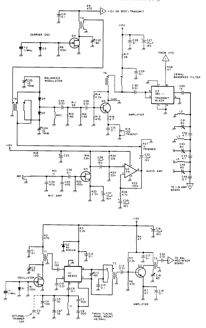
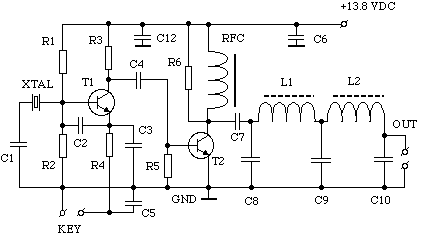
After this long helpful preface I think you must be able to understand now the issues around the Nexus 6 QRP transmitter, so let's get now on to the real stuff. Nexus 6 is currently under development so I will present you the transmitter step by step as I develop it. Let's start with the transmitter. The picture below shows the crystal oscillator and the oscillator PSU of the Nexus 6.

Crystal oscillator and oscillator PSU of the Nexus 6

The picture shows an ultra low phase noise low distortion crystal oscillator, along with it's power supply. This type oscillator has been discussed in detail with Charles Wenzel from Wenzel Associates, to define it's performance. You could expect a phase noise better than -150dBc from this circuit and this is far better than any PLL can do. That is why I use a crystal oscillator and not any other kind of PLL/DDS. The trick is not to overload the crystal and thus degrade it's high-Q. The crystal used in that place, acts as a filter too, which helps eliminating some of the unwanted signals at the output of the oscillator.

The 25pF variable capacitor is used to shift the frequency of the crystal a few tens or hundreds of Hz in order to achieve fine tuning. Do not shift the crystal frequency too much or the phase noise will be degraded. I have performed different power and frequency measurements on the oscillator to understand it's linearity, but since linearity may be depend on the specific crystal used, I would not like to present the measurement results here. In general, the oscillator is more linear at 7-18MHz and presents higher output levels, whereas the power level is a bit reduced at the low and high ends of the shortwave bands (160m and 10m).

As far as concern the mechanical construction, use a two-pole four-position panel switch to switch between different bands. Use a panel mount crystal holder in order to change crystals for different bands. Try to keep the leads lengths as short as possible. The crystal and the variable capacitor will be switched between the oscillator and the receiver filter using relays, but I will show this later on. For the time being, leave some empty space for a relay there. Use a panel mount air variable capacitor, preferably silver plated, in order not to degrade the Q of the crystal too much. If you cannot find silver plated capacitors use aluminum or nickel plated, but always use air dielectric ones. Warning, both poles of the variable capacitor must be insulated from the chassis. Additionally, connect the capacitor such as the pole that you touch with your finger is connected at the 22 Ohm resistor side and not at the oscillator side! If you do it the other way, the oscillator frequency will change a bit every time you touch the capacitor with your finger. Even if you use an insulating knob for the capacitor, it is a good idea to connect it as I mentioned.

The power supply of the oscillator is composed of a BC547 transistor and a 2N4401. The BC547 section behaves like a capacitor multiplier, multiplying the 100uF at the base of the transistor with the 100uF shunt capacitor, to give a total of 10000uF. This should suppress any potential hum, but to achieve a lower phase noise oscillator I have added the 2N4401 section taken out from Wenzel Associates.

System designers often find themselves battling power supply hum, noise, transients, and various perturbations wreaking havoc with low noise amplifiers, oscillators, and other sensitive devices. Many voltage regulators have excessive levels of output noise including voltage spikes from switching circuits and high flicker noise levels from unfiltered references. The traditional approach to reducing such noise products to acceptable levels could be called the "brute force" approach - a large-value inductor combined with a capacitor or a clean-up regulator inserted between the noisy regulator and load. In either case, the clean-up circuit is handling the entire load current in order to "get at" the noise. The approach of the 2N4401 circuit described here uses a bit of finesse to remove the undesired noise without directly handling the supply's high current.

The key to understanding the "finesse" approach is to realize that the noise voltage is many orders of magnitude below the regulated voltage, even when integrated over a fairly wide bandwidth. For example, a 10 volt regulator might exhibit 10 uV of noise in a 10 kHz bandwidth - six orders of magnitude below 10 volts. Naturally, the noise current that flows in a resistive load due to this noise voltage is also six orders of magnitude below the DC. By adding a tiny resistor, R, in series with the output of the regulator and assuming that a circuit somehow manages to reduce the noise voltage at the load to zero, the noise current from the regulator may be calculated as Vn/R. If the resistor is 1 ohm then, in this example, the noise current will be 10uV/1ohm = 10uA - a very tiny current! If a current-sink can be designed to sink this amount of AC noise current to ground at the load, no noise current will flow in the load. By amplifying the noise with an inverting transconductance amplifier with the right amount of gain, the required current sink may be realized. The required transconductance is simply -1/R where R is the tiny series resistor.

The 2N4401 circuit is suitable for cleaning up the supply to a low current device. A 15 ohm resistor is inserted in series with the regulator's output giving a 150 millivolt drop when the load draws 10 mA - typical for a low-noise preamplifier or oscillator circuit. The single transistor amplifier has an emitter resistor which combines with the emitter diode's resistance to give a value near 15 ohms. The regulator's noise voltage appears across this resistor so the noise current is shunted to ground through the transistor's collector. The noise reduction can be over 20dB without trimming the resistor values and the intrinsic noise of the 2N4401 is only about 1 nanovolt per root-hertz. Trimming the emitter resistor can achieve noise reduction greater than 40 dB.

http://www.neazoi.com/qrp/

60W RF Linear amplifier


The 60 Watt linear amplifier is simple all solid state circuit using power mosfet IRF840. The IRF series of power transistors are available in various voltage and power ratings. A single IRF840 can handle maximum power output of 125 watts. Since these transistors are used in inverters and smps they are easily available for around Rs: 20/-.

The IRF linear amplifier can be connected to the out put of popular VWN-QRP to get an output of 60 Watts. The circuit draws 700 ma at 60 Volt Vcc. Good heat sink is a must for the power transistor.

Alignment of the circuit is very easy. Connect a dummy load to the out put of the circuit. You can use some small bulb like 24V 6Watts as the dummy load. I have even used 230V 60Watts bulb as dummy load with my IRF840 power amplifier working at 120Volts. Adjust the 10K preset to get around 100 ma Drain current. I used gate voltage of 0.8V with my linear amplifier. A heigh gate voltage can make the power transistor get distroyed by self oscillation. So gate voltage must be below 2V and fixing at 1V will be safe.

Bifalar transformaer T1 is wound with 8 turns 26SWG on 1.4 x 1 balun core.
The coil on the drain of IRF is 3 turns 20 SWG wound on 4 number of T13.9 torroids (two torroids are stacked to form a balun core). The RFC at the Vcc line is 20 Turns 20 SWG wound on T20 torroid.

RF Power Amplifier 1.3W to 6W by 2SC1970


This amplifier is based on the transistor 2SC1970 and 2N4427.The output power is about 1.3W and the input driving power is 30-50mW.You can use other transistor as 2SC1971 and get much more output power.1.3W will still get your RF signal quit far and I advice you to use a good 50 ohm resistor as dummy load.Make sure it can take up to 5-10W, else it will be a hot resistor.You MUST use an antenna or 50 ohm dummy resistor while testing else you burn up the transistor.

RF Power Amplifier 1.3W to 6W by 2SC1970
In all RF system and specially in RF amplifiers, it is very important to have a stable power supply and making sure you won’t get any RF out on the power line. The Capacitor C12 and C13 will stabilise the DC power supply. L1, C10, C11 and L3 with C8, C9 will also prevent RF from leaking out to the powerline and cause oscillation or disturbances. L1 and L3 should be ferrite chokes or inductance’s about 1 to 10 uH.

Transistor Q1 will act as a buffer amplifier, because I don’t want to load the previous stage to much.The input RF signal is passin C1 and F1 which is a small ferrite pearl where the wire just passing through.F1 with C2 will act as an impedance matching for Q1.F1 can be substituted with a coil as L4, but in my test I found that the ferrite pearls gave best performances.L2 is nit a critical component and any coil from 2-10uH will do the job. Q1 will amplify the input signal from 50mW to about 200mW.Q1 can amplify much more, but It doesn’t need to do that because 200mW is good for the final transistor.If you want higher power you can decrease the resistor R2.

If you look at Q2 you will also find a ferrite pearl F2 at the base to emitter. This ferrite pearls is to set the DC voltage to zero and be a high impedance for RF signals. I wounded the wire 4 times around this small ferrite pearl. You can substitute it with a coil of 1uH or more.C4, C5 and L4 forms an input matching unit for the transistor. Not much we can do about that…At the output of the final transistor Q2 you will find 2 coils L5 and L6.
Together with C6 and C7, they form an impedance unit for the antenna and also for the transistor.

Sunday 13 March 2011

A simple 80 Meter CW Transmitter Using A 2N3904.

image


http://www.sparkbangbuzz.com/easy-ten/easy-ten.htm

EI9GQ's SIMPLE 80m TX


C1 = 47PF : C2, C3 = 1500PF : C4 = 0.01mfd : C5, C7 = 0.1mfd : C6, C12 = 0.047mfd : C8, C10 = 820PF : C9 = 1500PF : R1, R2 = 5K1 : R3, R5 = 100R : R4 = 180R : R6 = 1K2 : RFC = 22 MICROHENRIES (APPROX) : L1,L2 = 2.2 MICROHENRIES (21 TURNS ON T50-2) : T1 = 2N2369A : T2 = CB OUTPUT TRANSISTOR (2SC1237 OR SIMILAR) : XTAL 3.579MHZ (CHEAP COLOUR TV CRYSTAL) OR 3.560MHZ (QRP CW FREQUENCY)

This simple circuit will give about 1.2 Watts of output when powered from a 13.8VDC supply. If you don't have a 2SC1237, try any other 12V CB radio output transistor 2SC1969, 2SC1307 etc. The value of RFC is not critical, 10 turns on a high permeability ferrite toroid core works fine. I used a DPDT switch for the RX/TX switching, one pole for the aerial (antenna), the other pole to switch the 13.8V supply.

http://www.zerobeat.net/g3ycc/ei9gq.htm

Friday 11 March 2011

AM/FM/SW active antenna


This circuit shows an active antenna that can be used for AM, FM, and shortwave (SW). On the shortwave band this active antenna is comparable to a 20 to 30 foot wire antenna. This circuit is designed to be used on receivers that use untuned wire antennas, such as inexpensive units and car radios. L1 can be selected for the application. A 470uH coil works on lower frequencies ( AM ). For shortwave, try a 20uH coil. The unit can be powered by a 9 volt battery. If a power supply is used, bypass the power supply with a .04uF capacitor to prevent noise pickup. The antenna used on this circuit is a standard 18" telescoping type. Output is taken from jack J1 and run to the input on the receiver.

Micro Power AM Broadcast Transmitter


In this circuit, a 74HC14 hex Schmitt trigger inverter is used as a square wave oscillator to drive a small signal transistor in a class C amplifier configuration. The oscillator frequency can be either fixed by a crystal or made adjustable (VFO) with a capacitor/resistor combination. A 100pF capacitor is used in place of the crystal for VFO operation. Amplitude modulation is accomplished with a second transistor that controls the DC voltage to the output stage. The modulator stage is biased so that half the supply voltage or 6 volts is applied to the output stage with no modulation. The output stage is tuned and matched to the antenna with a standard variable 30-365 pF capacitor. Approximately 20 milliamps of current will flow in the antenna lead (at frequencies near the top of the band) when the output stage is optimally tuned to the oscillator frequency. A small 'grain of wheat' lamp is used to indicate antenna current and optimum settings. The 140 uH inductor was made using a 2 inch length of 7/8 inch (OD) PVC pipe wound with 120 turns of #28 copper wire. Best performance is obtained near the high end of the broadcast band (1.6 MHz) since the antenna length is only a very small fraction of a wavelength. Input power to the amplifier is less than 100 milliwatts and antenna length is 3 meters or less which complies with FCC rules. Output power is somewhere in the 40 microwatt range and the signal can be heard approximately 80 feet. Radiated power output can be approximated by working out the antenna radiation resistance and multiplying by the antenna current squared. The radiation resistance for a dipole antenna is 80*pi^2*(length/wavelength)^2 which yields about 0.2 ohms for a 3 meter dipole at a frequency of 1.6 MHz. Radiated power at 20 milliamps is about I^2 * R = 80 microwatts and for a grounded system with a single element whip antenna, the radiated power is about half that, or 40 microwatts.
Original scheme edited by Bill Bowden, http://www.bowdenshobbycircuits.info


Thursday 10 March 2011

2A Regulated PSU


By Nadisha 4S7NR

Main thing this works, Only thing you will have to find a sutable transformer that gives about 15V(2A) at your house hold power 220V or 110V.

VHF Regenerative Receiver


Submited By Nadisha 4S7NR

Looks very simple. But need bit experiance to build this receiver. It can be tuned from 140 to 150 Mhz covering the whole 2m band. This has a Super Regenerative detector. When properly tuned and aligned the receiver is very sensitive. The original author R.H.Longden writing in a Practical Wireless artical says that he could hear transmissions of 10 miles with a 6 inch wire antenna.

Receiver must be enclosed in an metel box and Tuning spindle should be fixed with a plastic knob. One should never try to construct this on IC boards or Vero boards.

L1 and L2 Coils should be wound using 18 SWG wire and L1 is only one turn where L2 has 4 turns (7/8 inch long). They are air wound on 1/2 inch diameter form. L2 should be next in-line to L1. Changing the turn spacing of L2 change the frequency. So you will have to experiment and find where it tunes. If you have an signal genarator - with in no time you will be in the business. L3 is not very critical, it has 30 turns of 26 SWG wire on a 1/4 inch diameter air core.

Once evry thing is okay, connect an audio amplifier, similer to LM386 and a sutable antenna to the receiver. Turn the 25k pot (Regen Control) where a strong hiss begins. This is roughly the correct posision. This hiss should cease when any signal of sufficiant strength is tuned in. Tune the 10pf tuning cap to search any stations or tune your signal genarator to see where the receiver is tuned. Once you know the place, adjust the coil. To increase the frequency, you will have to stretch the turns of L2.

http://www.qsl.net/qrp/rx/vhf-rx.htm

Wednesday 9 March 2011

80M CW Transmitter

image

CRYSTAL TESTER


Figure shows the circuit of a simple crystal tester. It switches on a light emitting diode (LED) if the crystal is working.

The crystal under test is placed in an oscillator circuit. If it is working, an RF voltage will be present at the collector. This is rectified (converted to DC) and made to drive a transistor switch. Applying current to the base causes current to be drawn through the collector, thus lighting the LED.

If an indication of frequency is required, simply use a general coverage receiver to locate the crystal oscillator's output. Note however that when testing overtone crystals (mostly those above 20 MHz) the output will be on the crystal's fundamental frequency, and not the frequency marked on the crystal's case. Fundamental frequencies are approximately one-third, one-fifth or one-seventh the overtone frequency, depending on the cut of the crystal.

The circuit may be built on a small piece of matrix board and housed in a plastic box. Alternatively, a case made from scrap printed circuit board material may be used. Either a selection of crystal sockets or two leads with crocodile clips will make it easier to test many crystals quickly. The RF choke is ten turns of very thin insulated wire (such as from receiver IF transformers) passed through a cylindrical ferrite bead. Its value does not seem to be particularly critical, and a commercially-available choke could probably be substituted.

The circuit can be tested by connecting a crystal known to work, and checking for any indcation on the LED. A shortwave transistor radio tuned near the crystal's fundamental frequency can be used to verify the oscillator stage's operation. Note however that this circuit may be unreliable for crystals under 3 MHz, and some experimentation with oscillator component values may be required.

The crystal checker also tests ceramic resonators. Other applications include use as a marker generator for homebrew HF receivers (use a 3.58 MHz crystal) and as a test oscillator for aligning equipment.

Figure Two:


Ten Steps to QRP Success

1. Use efficient antennas
A half wave dipole or better is preferred.

2. Know your capabilities - do not expect DX every time
It would be nice to work Europe with one watt to a mobile whip on forty metres, but do not expect such contacts to come easily (if at all). Instead, you should cast your sights a little lower and enjoy the closer-in contacts that are more achievable.

3. Have frequency-agile equipment
Many articles describe simple crystal-controlled QRP transmitters that can be put together in an evening. These are fun to build but frustrating to operate; 99 percent of such rigs sit on shelves, unused, gathering dust. Instead, use a VFO or 3.58 MHz variable ceramic resonator on eighty metres, or a VXO with at least a 10-15 kHz tuning range on the higher bands.

4. Use 'tail-ending' to advantage
When your signal is weaker than average (such as when operating QRP), 'tail-ending' is the most effective way of obtaining contacts. Simply tune across the band, noting the contacts that are ending. When all stations sign clear, call one of the stations. They will most likely reply to your call, even if only to give a signal report.

5. Have a quality signal
A transmitter that clicks and chirps is harder to copy at the other end than a signal from a clean and stable rig. This is particularly the case when the receiving station is using narrow CW filters.

6. On CW, know the relationship between your transmit and receive frequencies
It is possible for a station to miss your call if you are transmitting on the wrong frequency. Set direct conversion QRP rigs so that they transmit about 800 Hz below their receive frequency. Conversely, if calling CQ, tune around your normal receive frequency (with the RIT control) just in case a station is calling you on the wrong frequency.

7. Have an efficient transmit/receive switching system
A homebrew station that requires the operator to flick two or three switches to switch from receive to transmit is inefficient and may result in missed contacts (particularly during contests). Use just one T/R switch or experiment with the many break in and timing circuits available.

8. Use the best receiver you can afford
Most of the complexity in a QRP station is in the receiver. While simple receivers are fine for casual SWLing, active operating requires a somewhat better class of receiver. Aim for good frequency stability, adequate bandspread, reasonable selectivity, good strong-signal handling and an absence of microphonics. A well-built direct-conversion receiver should satisfy on all five counts for all but the most hostile band conditions.

9. Enter contests to boost your operating skills
Many people think that high power is necessary to participate in contests. This is untrue, particularly for the local VK contests. Contest rules are given in Amateur Radio magazine and on the WIA website.

10. Don't be afraid to call CQ
On bands such as ten metres, the band can be wide open, but no one would know as every body is listening. Call CQ, particularly when you have grounds for supposing the band is open, for example reception of beacons or 27 MHz CB activity. Automatic CQ callers using tape recorders, computers or digital voice recorders are particularly handy here.

One Valve CW transmitter


This transmitter was first constructed in 1987 and provided the author with his first 'real' rig, capable of distances of more than about 100 metres. It performed better than expected, with 250km contacts being commonplace and 2500km being occasionally possible.

It consists of a 6GV8 valve, common in the many valve TVs that were rusting in rubbish tips at the time. Unlike some slightly simpler designs, it is a two stage circuit, the triode section being used for the oscillator and the pentode as the power amplifer. With a high tension of about 200 volts power output of about 3 watts could be obtained on 3.5 MHz.

It will work with the cheap 3.58 MHz crystals, but you won't get many contacts up there – better to invest in a lower frequency crystal – eg 3.530 MHz or so. A VXO is not provided – these do not usually provide much shift with 3.5 MHz crystals. However if you wish to add one, wire an inductor (approx 6.8uH) in series with the crystal and add a variable capacitor from point 'A' to earth.

A circuit for a power supply is not included. The one used for this project is based on a transformer from an old valve radio. Use a bridge rectifier and electrolytic capacitor (rated at 350v or so) for smoothing. However as the current drawn is low, even a single 1000v diode will work as the rectifier in this circuit.

Like nearly all valve circuits, this transmitter uses lethal voltages. It should be fully enclosed so that no high voltage points can be touched by the operator. A metal chassis, such as a cake tin is suitable.

To test, insert a crystal, wire a small light bulb (eg dial light) across the antenna terminals and press the key. Adjusting the Tune and Load controls should cause the light to glow quite brightly. Plate current should be around 30-50mA. For the transmit/receiving switching, either have the receiver connected to a separate antenna or use a switch or relay to switch the antenna over.

circuit of 1 valve transmitter

40M VFO


clip_image002

clip_image004

N4UY 40M RF Power amplifier


clip_image002

This 40 meter amplifier posted Is handy for boosting the power of rigs running a few hundred milliwatts, and can put out 2 or 3 watts.

The RF enters through a 0.1 uF cap and a small ferrite bead to the PA transistors. A 2 uH inductor provides a DC return for the bases. 12 volt is applied to the collectors through an 8 uH choke. A 47 pF electrolytic cap and 0.1 pF cap bypass unwanted signals from the V+ source to ground.

L Match Tuner for End-Fed wire antenna


clip_image002

In this tuner. a variable inductor made bv mutual coupling between two coils of near equal inductance is used as the L match inductor. The object is to have a variable inductor with no taps or rollers. These coupled coils, LI and L2 are connected in series (see Figure) to get total inductance.

A reverse switch connects the two coils either for additive or subtractive M to accomplish a wide range of total L. With LI = L2 = 10 uH and K = 0.8 the range is about 4 to 36 uH. One coil is wound on the plastic case of

a 12 ga empry shotgun shell and the other on a 20 ga empty shotgun shell . The winding is #23 magnet wire so that the outside diameter of the 20 ga coil slides nicely into the 12 ga shell to allow variable coupling by sliding the smaller coil in and out of the larger coil.

1. Use a low base 20 ga empty shotgun shell and drill out the primer end to clear a 114 inch screw.

2. Take a 1/4-20 nylon hex nut and glue it over the hole just drilled. This gives the shell a threaded nut that will run on a lead screw to move this coil in and out of the 12 ga shell.

3. In preparation for winding the coil cut off and discard about 318 inch of the crimped end of the 20 ga plastic so that a well formed coil form remains.

4. Locate and drill a 1132-inch dia hole in the plastic about 114 inch from the end just prepared. This is for the start of the $23 magnet wire winding.

5. Locate and drill another 1132" dia. hole in the plastic about 7116 inch from the fust hole toward the base. This allows 15 turns between the holes from start to finish, Drill a 1W-inch hole close to the base that will serve to bring both ends of the winding out for connections clear of the sliding fit. .

6. Wind 15 turns of #23 magnet wire between the two 1132 dia holes. Start with one end into a 1132 dia hole, into the shell and out the 118-inch hole. When 15 turns are on, put the end into the nearby 1132- inch hole, down the center of the shell and out the 118-inch hole pulling the wire tightly to maintain tight turns.

7. Take a 12 ga shell, cut the crimped end off to make a uniform coil form and wind on 13 turns of #23 magnet wire. No holes are used for the start and finish of the winding so tape must be used hold the winding and dress the leads. Clear fingernail polish may be useful as well.

8. A 1/4-20 x 2 inch nylon machine screw along with an extension of 114 inch wooden doweling is used to make the lead crew shown in the diagram in Figure

Noice source


clip_image002

A broadband noise source is useful for testing purposes. This circuit gave a reasonably flat output up to 30 MHz when checked with a general coverage receiver. The output impedance is about 50 ohms. It's basically a zener diode used as a noise source with a broadband RF amplifier. I think the higher power zeners give more noise, which is why I used a 1W device. The zener voltage isn't critical, of course; use whatever you have around 6V. The 4:l transformer is 8 bifilar turns on a SiemensEPCOS B64290P37X33 ferrite toroid. An FT37-43 could be used.

FM Superregenerative Receiver

The oscillator coil is made from five turns of 0.8 mm (ideally, silver plated) copper wire on a diameter of 8 mm. Short connections are essential, especially to the tuning capacitor: we soldered a trimmer directly to the ground plane. The second coil in the circuit consists of 20 turns of 0.2 mm enamelled copper wire wound on a 10 kÙ resistor. The rest of the circuit is constructed as shown in Figure.

image

The antenna should not be too long, as otherwise the circuit may cause interference: the superregenerative circuit is also a transmitter! Nevertheless the circuit is very sensitive and operates perfectly satisfactorily using a 10 cm length of wire for an antenna. The headphones should ideally have an impedance of at least 400 Ù. The circuit will work with 32 Ù stereo headphones, but the output will not be as loud. It is important to use a transistor designed for radio frequency use (such as the BF494) as it is difficult to get the circuit to work using an ordinary audio frequency device such as the BC548B.

Tuesday 8 March 2011

DPN 7MHZ QRP Transmitter

image

R1                            1   100R,Resistor (USA Style)
R2                            1   10K,Resistor (USA Style),..
C3                            1   10nf,Capacitor
Q1                            1   2N2222,Bipolar Transistor
L1                            1   30t on 1/2inch PVC pipe,Inductor,..
R3                            1   330R,Resistor (USA Style)
C2                            1   330pF,Capacitor
R4                            1   33K,Resistor (USA Style)
C4                            1   365pF,Capacitor Variable
Q2                            1   BD139,Bipolar Transistor
J1                            1   COAXJ,Coax Jack
G1                            1   GND,Chassis ground
T1                            1   Modulation Transformer,Dual Sec. Transformer w. pins,P
T2                            1   Shortwave,Transformer,4
C1                            1   VC1,Variable Capacitor
X1                            1   XTAL,Crystal

Output power of this transmitter is around 0.8 watts sufficient enough for qrp operation.This circuit uses easily available old radio junks like shortwave osc.coil , audio output transformer, 2J variable gang condensers, which makes your job easy. If you have any suggestions or modification ideas please let me know at bcdxer@hotmail.com.

Thanks

455 KHZ Beat Frequency Oscillator

image

This simple BFO can be useful to resolve SSB signal in your shortwave radio receiver. Keep the wire from bfo near to ur receiver when you logged a ssb signal and tune the core of IFT till better audio.

Low Cost ATU for QRP rigs

image

The circuit shows simple low cost ATU for QRP transmitter projects. The coil is wound on a 12mm ferrite rod, which can be junked from old radio receivers.The wire will be 20swg and  the winding should occupy 4cm long.VC1 and VC2 are 365 pf Variable condensers used in radio receivers.

Simple 80M transmitter

image

image

Simple 160M Novice transmitter

image

Simple audio S meter

image

21MHz DSB Transmitter


image

See the circuit! DSB transmitter has no need of a crystal filter. It does not need a frequency transverter. It is easy to make. And it can make QSO with normal SSB stations. Therefore DSB is best modulation for the amateur radio builder. The mic amplifier makes the audio signal stronger. The VXO oscillates a 10.6MHz signal. This is doubled by the amplifier of the TA7320 IC. These two signals are modulated by the DBM of the TA7320. There comes the 21MHz DSB signal. HF amplifier makes this signal to 250mW.

3 transistor 50MHz DSB transmittor


image


Input transformer of this circuit is an audio transformer. The output transformer of this modulator is made by coil. This modulator is understood as a pair of base grounded amplifier for the carrier. But two output of collector is connected as other side of a coil. Therefore the carrier is balanced and can not be out for the antenna connector

2SC1957 linear AMP

image

Single transistor FM transmitter

image

This is oscillator using a crystal. This oscillator makes the wave 5 times of the crystal. 19.2*5=96MHz. And the frequency is modulated by the audio signal came from the base of the transistor.Do not joint the antenna wire for this transmitter! The frequency of this transmitter is stable than self oscillator. But it is not so stable as a normal crystal oscillator. The antenna wire changes the frequency.

Simple L-MATCH ATU for End-fed wire antenna

image

Super simple CW transmitter

image

The figure shows super simple CW transmitter with bare minimum components

80M QRP 3 watts Transmitter for novices

image

Ramsey HR-40 CW/SSB Direct Conversion Receiver

image

Schematic diagram for the Ramsey HR-40 CW/SSB Direct Conversion Receiver. Ramsey Electronics Inc

Figure shows the circuit for the HR-40 Direct Conversion Receiver for 40 meters. Here’s how this circuit works. The incoming signal from the antenna is coupled through C5 and the RF gain control R1, to antenna input transformer L1. (A 10.2-MHz IF transformer, detuned to cover the 40-meter band, can be substituted.) This “tuned” transformer peaks the  desired signal and applies it to the NE602’s mixer section. The shielded oscillator coil, L2, along with varactor diode D1, R2, R5, C1, C2, C3, and
C4, form an oscillator network with the NE602’s internal oscillator. Rotating R2 varies the oscillator’s frequency over a tuning range of about 250 kHz. The NE602 mixes the incoming RF signal with the signal from the internal oscillator to produce an audio signal at Pin 4. The output audio signal is coupled to the LM 386 audio amplifier via coupling capacitor C8 and volume control R3. Capacitor C9 boosts the voltage gain of the LM386 to about 50. The high-level audio output is coupled from Pin 5, U2, to external headphones or a low impedance (4 to 8 ohms) speaker through coupling capacitor C12 and output connector J2.NE602.

An internal 9-volt transistor battery (or an external power source of about 9–12 Vdc, 60 mA) is used to power the HR-40. Note that zener diode D2, along with C10 and R4, form a 6.2-Vdc voltage regulator network to improve stability of the NE602’s internal oscillator circuit.

A simple crystal receiver for the beginner

image

A simple crystal receiver for the beginner

Ramsey Electronics Model QRP-40 CW Transmitter

image

Schematic diagram for the Ramsey Electronics Model QRP-40 CW Transmitter. This easy-
to-build CW transmitter provides about one watt of output RF power in the 40-meter
band. Ramsey Electronics Inc.

Code practice oscillator

CPO

Schematic diagram for code practice oscillator circuit using the Signetics NE555 IC
Timer.

Cigar·lighter polarity Tester

image

Before you plug your equipment into the cigar lighter of your new (or an unknown) car, it's a good idea to test the lighter polarity. Fig shows a simple means of doing this. The circuit tests for a center positive condition at the lighter; if the lighter is powered, and + 12 volts is connected to its center contact, DSllights. Carry this gadget with your "pluggable" 12-V gear; it could save your transceiver from a quick demise.

Thursday 3 March 2011

CRYSTAL TESTER

This circuit will test crystals from 1MHz to 30MHz.  When the crystal oscillates, the output will pass through the 1n capacitor to the two diodes. These will charge the 4n7 and turn on the second transistor. This will cause the LED to illuminate.

XtalTester

Simple circuit helps high-power VHF transceivers cool themselves

image


Some compact, high-power VHF transceivers get very hot when transmitting and can benefit from forced-air cooling. The simple circuit shown in Fig helps such radios cool themselves. It senses RF leakage from coaxial cable and turns on a cooling fan whenever the radio is transmitting.

Inductor Ll consists of 10 turns of insulated hookup wire-H2O to 24-wrapped tightly around the coax and taped into place. You need not alter the coax in any way. (Although my test circuit worked well with 10turns, your version may work better with more or less turns. You can optimize Ll by connecting a voltmeter across Rl and adjusting Ll for a peak read ing while transmitting.) Dl rectifies the signal. Cl filters the resulting de, which is applied to Ql's base to turn QI on. RI keeps QI turned off during no-drive periods by pulling Ql's base to ground.

The circuit has other uses. For instance, it could drive a TRANSMITTER ON indicator to warn you that your mobile mike is jammed between your car's seats with its push-to-talk button held down. Or, combined with a timer, it could serve as part of a transmitter-time-out warning circuit.

Author - Jay F. Hamlin, WB6HBS