Series-tuned Clapp oscilla-torusing high-impedance JFET at has good fre-quency stability. Diode stabilizes bias. Air variable C1 provides frequency spread of exactly 100 kHz. L1 is 25-58 μH slug-tuned (Miller 43A475CBI). L2 is 10-18.7 μH slug-tuned .
Saturday, 19 March 2011
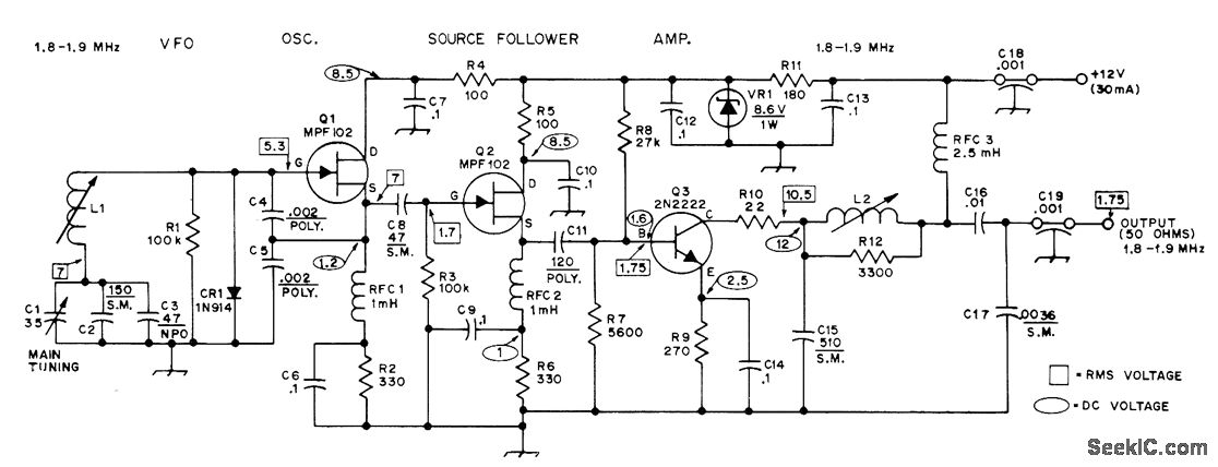
1.8-1.9 MHz VFO
80-M AMATEUR RADIO TRANSMITTER
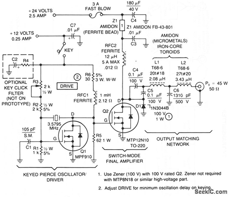
This transmitter consists of a keyed crystal oscillatoridriver and a high efficiency final, each with a TMOS Power FET as the active element. The total parts cost less than $20, and no special construction skills or circuit boards are required.
The Pierce oscillator is unique because the high CRSS of the final amplifier power FET, 700 - 1200 pF, is used as part of the capacitive feedback network. In fact, the oscillator will not work without Q2 installed. The MPF910 is a good choice for this circuit because the transistor is capable of driving the final amplifier in a switching mode, while still retaining enough gain for oscillation.
To minimize cost, a readily-available color burst TV crystal is used as the frequency-determining element for Q1.An unusual 84% output efficiency is possible with this transmitter. Such high efficiency is achieved because of the TMOS power FET's characteristics, along with modification of the usual algorithm for determining output matching.
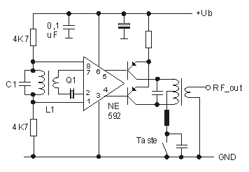
RF Power Oscillator
You can build a power oscillator with an NE592 and some additional parts. Depending on the crystal frequency, RF power generation in the range of 1 to 30 MHz is possible. The parallel resonant circuit C1/L1 must be tuned exactly to the crystal frequency. For final transistors one can use two 2N3906 or BS250 (see QRP push-pull amplifier). RF power output can be adjusted from 20 mW to 1.5 W by varying a common emitter resistor in the push-pull stage.
Do not use this circuit as a transmitter. When keying the NE592 power supply (pin 3) frequency variation (chirp) occurs. If you insist on transmitting with this circuit, then switch the final transistors directly. To do this put a 10 uH choke in series with the key and a 0.1 uF capacitor in parallel. Disadvantages of this circuit are the NE 592 quiescent current (18 mA), the continuously working oscillator and the hard keying.
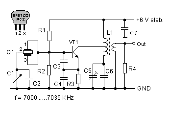
VFO with Ceramic Resonator
A 7 MHz oscillator with a variable crystal oscillator (VXO) operates very stably, but it allows only a small frequency variation (approx. 5 kHz). In contrast, a VFO with an LC resonant circuit can be tuned over a range of several hundred kHz, but its frequency stability will depend upon its construction. The use of a ceramic resonator as frequency-determining component fulfills both requirements. The following oscillator circuit, which uses a ceramic resonator, offers a tuning range of 35 kHz with good frequency stability. The somewhat unusual resonant LC circuit at the collector of VT1 has two functions. It improves the shape of the output signal and at the same time compensates the amplitude drop starting at approximately 7020 kHz. The transfer characteristic of the ceramic resonator gives this effect. The resonant LC circuit must be adjusted for maximum output amplitude (2Vss) at 7035 kHz. The oscillator needs a regulated voltage of +6 V for proper operation.
The resonant LC circuit can also be tuned to the second, third or forth harmonic. For an improved signal shape however, an extra tuned amplifier stage is necessary. With this adjustment the oscillator is capable for use on 20 meters (14000-14070 KHz), 15 meters (21000-21105 KHz) or 10 meters (28000-28140 KHz).
Push-pull Linear Amplifier with NE592 Driver
Transformer T1 matches the relatively low impedance present at the VFO FET gate to the balanced inputs of the NE592. With a unipolar power supply, it is necessary to bias both inputs to roughly one-half of Vcc. Below, we have shown both inputs tied to +6 VDC, conveniently available from the VFO. If 6 volts were not available, we would employ a scheme identical to the "IF amplifier" shown earlier, with Vcc split in half with 2 4,7K-ohm resistors in a divider configuration, applied to both inputs. Normally, stage gain is determined by the value of a resistor between pins 2 & 7. Bench tests reveal better output symmetry, however, if we replace this resistor with a 1 nF capacitor.
Approximately 8 volts of RF drive is available at pins 4&5 if we don't load it too heavily. This is sufficient to drive a pair of 2N3906 PNP transistors in push-pull to roughly 1,5 watts output with excellent efficiency. With bias provided by the NE592, the output transistors are operated in their linear region. Push-pull operation provides inherent suppression of even-order harmonics (2f, 4f, etc.), thereby simplifying our output network design (not shown). T2 is a T44-2 toroid with 5 bifilar primary turns and a single 5 turn secondary. C1 is around 270 pF (for 10 MHz), and should be adjusted to resonate the primary of T2 to signal frequency.
Fig - Schematic of the push-pull final (Pin designations are for the 8 pin DIP package)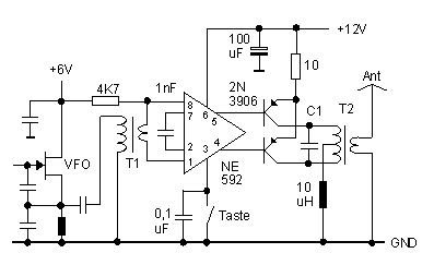
A tuned transform tank does not like to see a severely reactive load. An antenna tuner or some other means of cancelling reactance and transforming impedance must be employed if the load departs significantly from 50+j0 ohms. Broadband transformers, on the other hand, are inherently less sensitive to mismatch because of their low Q, but must be backed up with an effective harmonic suppression filter to achieve acceptable spectral purity. A single pi-network should do it. A low Q parallel-resonant circuit (low L, high C) was also tried, with acceptable results.
Subscribe to:
Comments (Atom)